
Contents
Weekly Thesis
Front-End Wafer Fab Equipment (WFE)
Metrology, Inspection, and Test
Advanced Packaging Equipment and Critical Materials
Companies, Orders, and Capex Validation
Debates, Counter-Evidence, and Next Week's Watchlist
Leading-edge fab expansions continue to anchor robust semiconductor equipment demand, with chipmakers pulling forward their procurement planning. However, lengthening component lead times and delayed glass substrate qualifications are widening the gap in revenue conversion timelines across different subsegments. We favor suppliers actively resolving equipment delivery bottlenecks and high-volume manufacturing (HVM) testing challenges, though conviction must remain anchored in firm order intake, site acceptance tests (SAT), and qualified yields.
Weekly Thesis
Capex sentiment across semiconductor equipment remains constructive, but alpha hinges on which vendors can convert shipments into qualified, productive fab capacity on schedule. This week’s developments—TSMC’s parallel leading-edge node expansions, SK Hynix pulling forward supply chain coordination, and collaborative advances in optical-electrical test—reinforce structural demand across front-end capacity, delivery readiness, and advanced packaging upgrades. While these catalysts explain why chipmakers are sustaining elevated capex, they do not resolve the timing of quarterly revenue recognition for OEMs.
On the demand side, the most notable shift is customers extending their planning horizons. Industry checks indicate that SK Hynix intends to lengthen the rolling demand forecasts shared with equipment suppliers from the historical 6–12 months out to two to three years (N+1 and N+2). While earlier visibility helps toolmakers secure long-lead components and allocate capacity, rolling forecasts remain subject to revision and must not be conflated with non-cancellable backlog.
The supply-side picture is more complex. Supply chain reports point to stretching tool delivery lead times at Applied Materials, ASML, and Lam Research, driven by tightening subcomponent supplies. For vendors with solid order backlogs, this signals that customers are eager to secure queue positions earlier; yet for near-term financials, parts shortages threaten shipment schedules. Tool-level delivery execution is increasingly becoming a prerequisite for validating backlog quality.
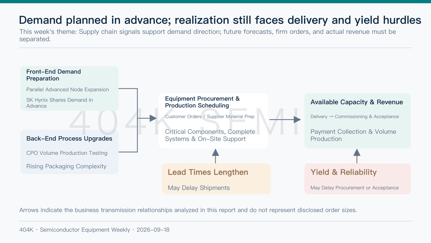
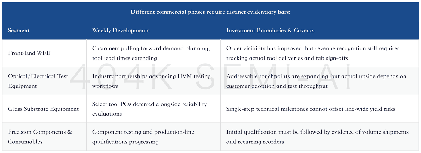
In back-end equipment, opportunities are more tangible but demand strict distinction across commercialization phases. SENKO, Advantest, and VIAVI are advancing HVM testing for co-packaged optics (CPO) modules, demonstrating that the ecosystem is tackling real-world measurement repeatability, optical interface coupling, and test throughput. In contrast, Samsung Electro-Mechanics (SEMCO) has reportedly deferred purchase orders for select through-glass via (TGV) tools. Robust secular demand for advanced packaging can readily coexist with procurement pauses in specific unproven process flows.
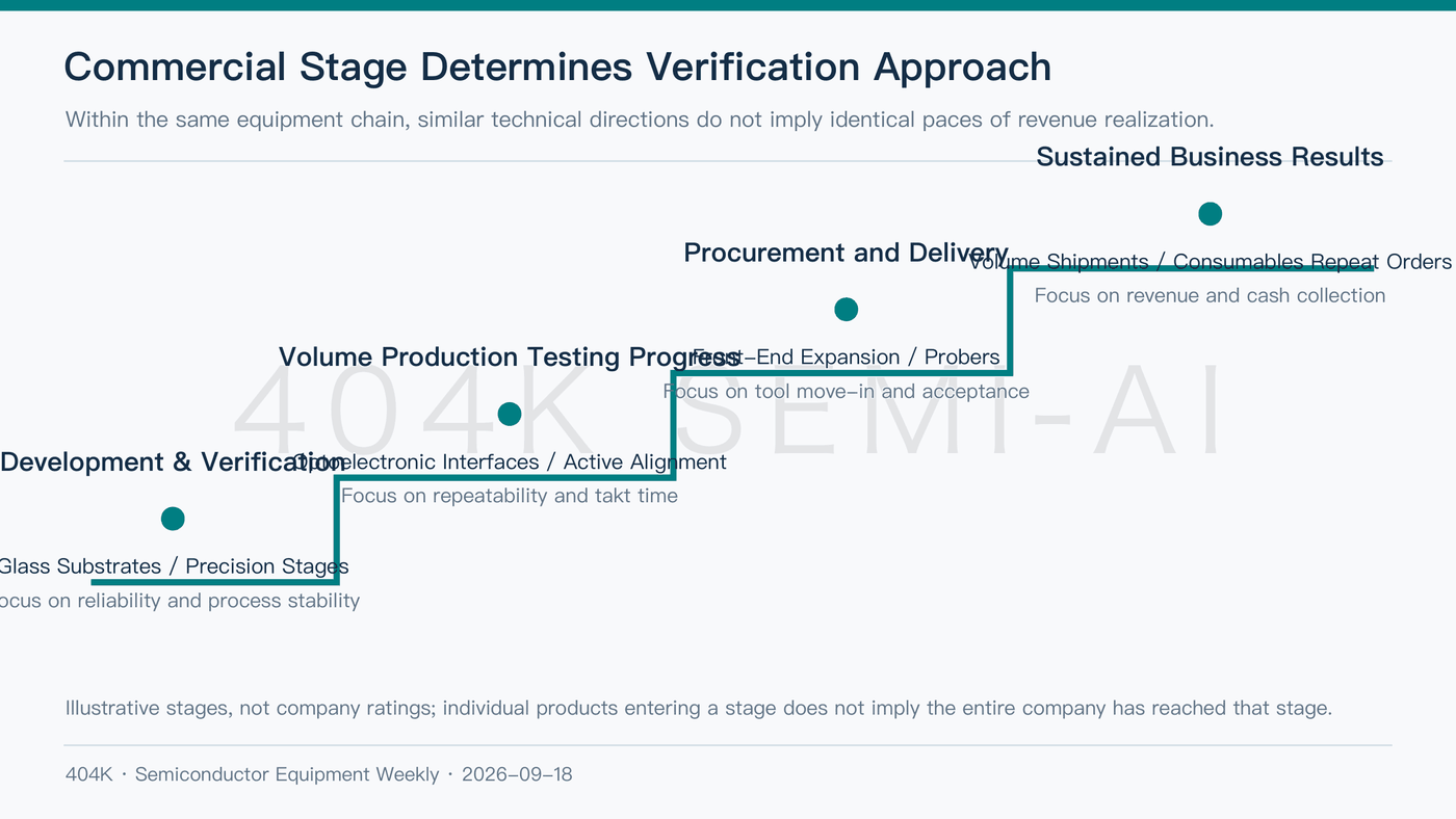
Our current investment hierarchy prioritizes: (1) mature tools with clear demand and trackable delivery schedules, followed by (2) tools undergoing customer qualification, and lastly (3) early-stage roadmaps. This hierarchy reflects revenue visibility rather than terminal technological value. Sampling tools that cannot demonstrate stable high-volume yields remain trapped in low-volume R&D; revenue, whereas mature tools facing component shortages can see order momentum decouple from sluggish physical shipments.
Front-End Wafer Fab Equipment (WFE)
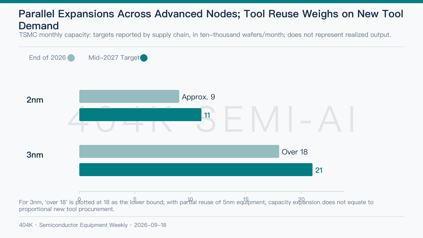
Leading-edge WFE demand is supported across multiple concurrent nodes; capacity additions at next-gen nodes do not imply the immediate obsolescence of prior nodes. Supply chain checks indicate TSMC is planning simultaneous expansions across its 2nm (N2) and 3nm (N3) footprints. Cost premiums, initial capacity allocations, and yield ramps at N2 prevent an immediate, wholesale customer migration, preserving elevated fab utilization at established nodes.
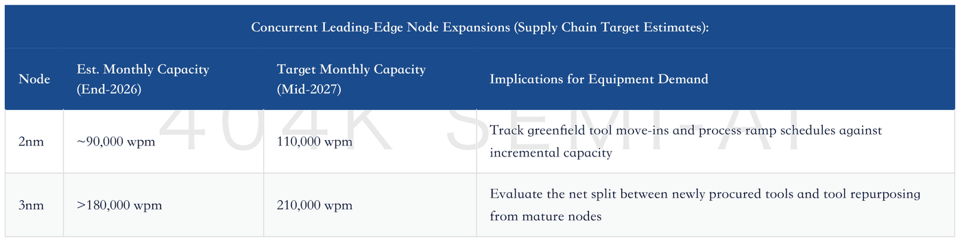
While these targets support constructive macro WFE sentiment, they are insufficient for modeling vendor-level order intake. Crucially, supply chain feedback notes that TSMC is repurposing select 5nm tools for 3nm lines. Tool conversion expands effective capacity without generating commensurate greenfield POs. When modeling WFE revenue from wafer capacity growth, analysts must adjust for tool reuse rather than naively multiplying target wafer capacity by a static capex-per-wafer metric.
More actionable indicators include whether foundries are expanding total tool quantities, locking in delivery slots earlier, and bringing tools on-line without delays. If foundries boost output primarily through line optimization and tool conversions, installed base services and modification upgrades will benefit, but new equipment bookings will lag headline capacity growth.
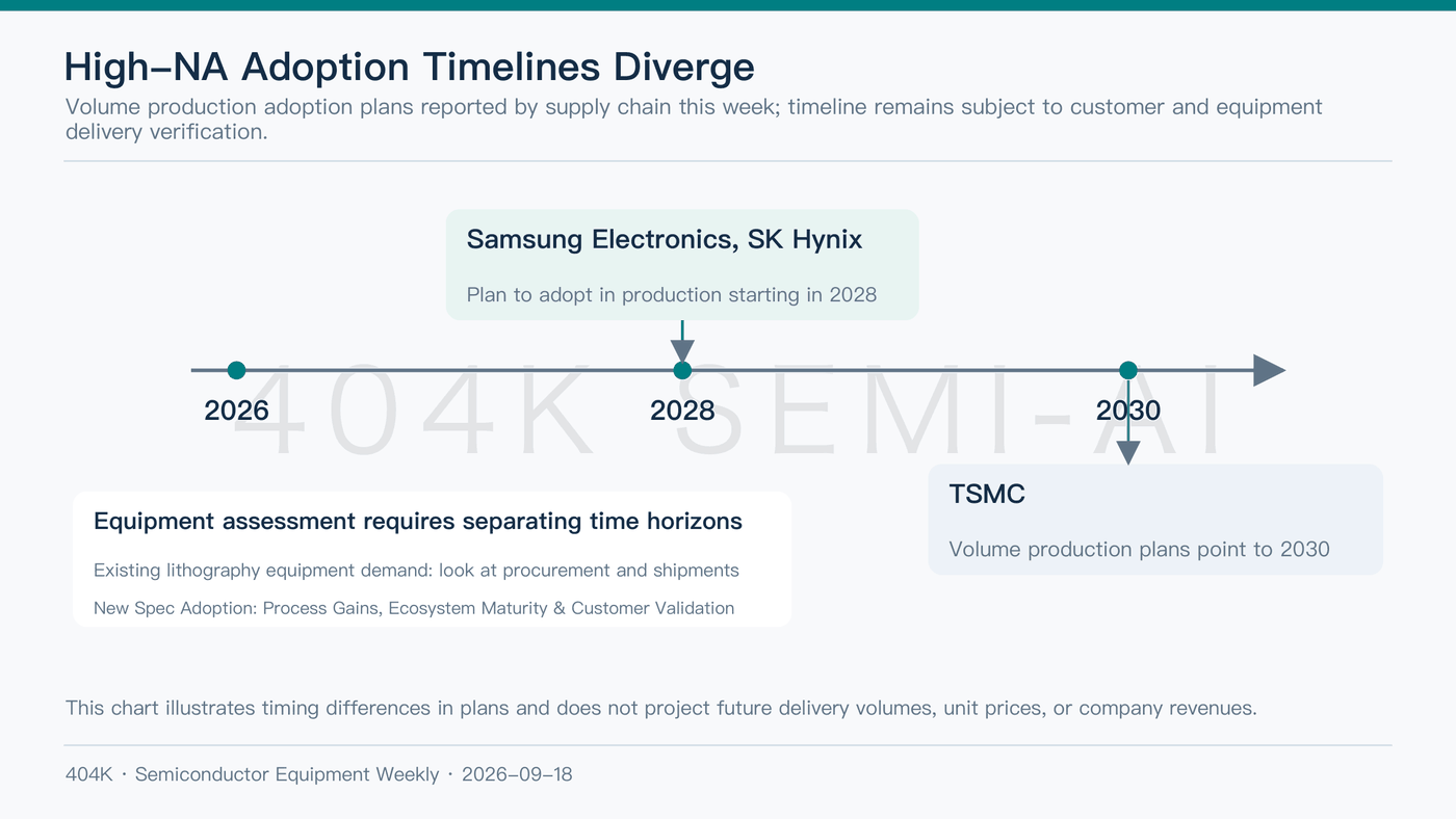
Diverging High-NA EUV adoption schedules underscore that cost economics and manufacturing readiness continue to dictate foundry and memory roadmaps. Industry checks regarding ASML this week suggest that Samsung Electronics and SK Hynix plan to integrate High-NA EUV into production starting in 2028, whereas TSMC’s HVM insertion timeline points to 2030. These remain strategic roadmap targets rather than committed HVM deployments.
ASML’s structural opportunity spans both advanced logic and DRAM; focus must not rest solely on a single logic foundry. Cantor’s bullish stance on ASML this week is premised on a rebound in lithography capital intensity, sustained DRAM node transitions driving EUV tool procurement, and expanding gross margins. However, these institutional hypotheses require validation through quarterly bookings and execution before earnings growth can be considered de-risked.
The divergence primarily reflects timing. Migrating to next-generation lithography requires proven wafer-level cost benefits and a fully matured ecosystem (resists, pellicles, masks). Delayed insertion by select customers does not prove structural demand destruction for lithography; conversely, published long-term roadmaps do not imply near-term order upside. Investors should decouple baseline Low-NA EUV tool demand from long-dated High-NA insertion schedules rather than blending them into a single monolithic growth profile.
Lengthening component lead times are shifting the primary bottleneck in equipment fundamentals from customer demand to supply chain execution. Channel checks indicate that lead times for select deposition equipment components have stretched from roughly 4 months to up to 10 months, with packaging equipment components facing similar delays. While these peak lead times illustrate localized bottlenecks rather than fleet-wide averages, they warn against assuming uniform revenue conversion across OEMs.
