
Contents
Weekly Executive Summary
Front-End Wafer Fab Equipment (WFE)
Metrology, Inspection, and Test
Advanced Packaging Equipment and Key Materials
Distinct Metrics Within the Forecast Warrant Separate Evaluation
Company, Order, and Capex Verification
UBS Projects Annual Increases in WFE Spending; Actual Procurement Cadence Remains Subject to Verification
Key Debates, Counter-Theses, and Next Week's Watchlist
Thesis Verification Depends on Observable Catalysts
Tool demand is expanding across leading-edge foundry nodes, packaging, and test, yet a substantial gap remains between capacity forecasts, technical qualifications, and confirmed purchase orders. This week, we see the most compelling opportunities in spending driven by rising process step counts and mass-production bottlenecks. However, monetization velocity hinges on customer qualification, tool orders, and capex execution—not paper capacity targets.
Weekly Executive Summary
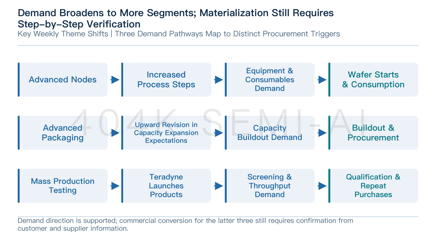
The most meaningful development for semiconductor equipment this week is that customers have more concrete reasons to invest. TSMC’s leading-edge nodes are driving incremental demand for etch, deposition, chemical mechanical planarization (CMP), and inspection/metrology; UBS revised up its advanced packaging capacity forecasts; and Teradyne rolled out a mass-production test system for MicroLEDs. These represent rising process complexity, expanding packaging footprints, and broader test coverage, respectively—supporting the continuing dispersion of equipment demand across the value chain.
The timeline for these catalysts to translate into revenue varies considerably. Teradyne has commercial hardware ready, while some of Samsung Electronics' capacity additions remain under review, and hybrid bonding and glass substrates still face validation hurdles. Investment decisions should follow a clear chain of verification: identifying the customer’s problem, confirming budget approval, verifying supplier qualifications, and pinpointing when orders materialize. Conflating technological progress with immediate cyclical upturns risks overestimating revenue ramp velocity.
For wafer fab equipment (WFE), the primary focus is process node migrations and actual fab disbursements; for packaging equipment, it is physical capacity buildouts and roadmaps; for inspection and test, the litmus test is solving real-world yield, binning, and throughput bottlenecks. The most actionable incremental data next week will be whether this demand translates into actionable backlogs for equipment makers, rather than yet another long-term TAM forecast.
Broadening demand also introduces market-share dispersion. Samsung Electronics reportedly incorporated wafer-to-wafer (W2W) hybrid bonding into its next-generation DRAM roadmap. Separately, reports indicate that Samsung Electronics and SK Hynix are evaluating alternative suppliers alongside Besi. The former signals a technology shift, while the latter reflects vendor diversification. An expanding addressable market does not guarantee that incumbent vendors will capture incremental orders at their historical share.
Similarly, ramping leading-edge nodes can drive both greenfield tool purchases and higher consumable utilization on existing lines. Tool sales, recurring consumables, and engineering validation services follow distinct revenue trajectories. In the near term, investors should focus on utilization trends across active production nodes, while longer-term architectural shifts must await customer qualifications and formal capex commitments.
While these developments establish a clear framework for tracking the sector, they are not yet sufficient to rank earnings visibility across equipment makers with precision. Priority should be given to segments backed by tangible commercial hardware, concrete customer milestones, and confirmed purchase orders or utilization data. Where companies offer only architectural roadmaps and market optimism, we advise staying observant until commercial execution catches up.
Front-End Wafer Fab Equipment (WFE)
Leading-edge nodes drive tool demand primarily because each wafer requires a higher number of processing steps. Reports indicate that TSMC’s 2nm gate-all-around (GAA) architecture demands significantly more etch, deposition, CMP, and metrology/inspection steps than preceding FinFET nodes. The commercial implication is straightforward: even with flat wafer starts, tool utilization and consumable run-rates can increase.
However, this dynamic cannot be generalized across all tool categories. Beneficiaries vary depending on where steps are added within the flow, and throughput gains on newer tools can partially offset the total unit count required. Evaluating tool orders requires analyzing incremental process steps, the fungibility of existing fleets, and the extent of additional inspection required for yield optimization. Relying solely on node nomenclature upgrades provides little visibility into actual revenue upside for equipment vendors.
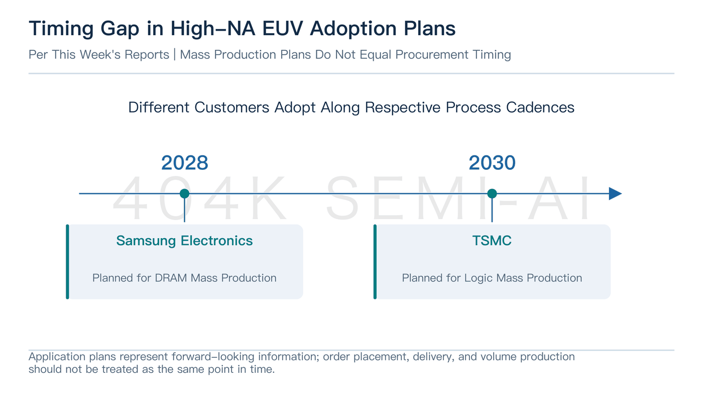
The divergent deployment timelines for High-NA EUV lithography underscore that customer investments remain asynchronous. Reports this week suggest Samsung Electronics plans to deploy High-NA EUV in high-volume DRAM manufacturing starting in 2028, whereas TSMC targets 2030 for leading-edge logic. These are company-specific roadmaps that should neither be extrapolated into synchronized industry-wide capex nor booked directly as current ASML order flow.
Samsung Electronics' base die requirements offer a nearer-term window into equipment demand. Driven by HBM4 adopting 4nm base dies, relevant fabrication lines are reportedly running at full capacity, prompting the company to evaluate capacity expansion. Because base dies handle high-speed data exchange with host compute silicon, surging demand could trickle down into logic process equipment. The critical next step is whether "evaluating expansion" crystallizes into formal budget approvals and procurement schedules.
However, high fab utilization alone does not guarantee a high-return capacity expansion. Other reports highlight that leading-edge yields, legacy contract margins, and new fab construction costs remain operational headwinds for Samsung Electronics. If debottlenecking existing capacity can satisfy incremental demand, new tool procurement could fall short of market expectations. Conversely, if yield ramp challenges persist, capex budgets may be channeled into process remediation rather than broad-based capacity expansion.
Mature nodes are currently seeing utilization and pricing improvements rather than confirmed new tool orders. UMC’s commentary regarding potential 2027 foundry price adjustments is predicated on sustained tight supply-demand conditions. Increased demand for PMICs, sensors, and microcontroller/logic units can first lift utilization on installed capacity; only when order durability and ROIC become unambiguous will this justify upgrading the thesis to a fresh wave of capacity expansion.
