
目录
Weekly Assessment
Front-End Wafer-Fabrication Equipment
Metrology, Inspection and Testing
Advanced Packaging Equipment and Critical Materials
Companies, Orders and Capital Expenditure
Debates, Counterevidence and Next Week’s Watchlist
Equipment investment is broadening into testing, inspection and advanced packaging. Follow-on orders carry more weight than distant capacity expansion plans, but customers’ willingness to keep buying still depends on whether installed tools consistently produce good chips. Next week, focus on deliveries, qualification and test efficiency, and avoid treating technology roadmaps as revenue before they materialize.
Weekly Assessment
The most significant shift this week is customers’ willingness to spend more on manufacturing to reduce the cost of scrapping expensive chips. From wafer testing to post-packaging inspection, equipment value increasingly depends on detecting defects early, shortening test times and ensuring smooth transitions between process steps. Leading-edge capacity continues to expand, but wafer-fab additions alone no longer adequately capture equipment suppliers’ growth prospects.
The evidence spans several stages of commercial maturity. Aehr received follow-on orders for wafer-level burn-in systems; FormFactor discussed additional probe-card capacity and customer adoption of photonics testing; and Applied Materials management said at a Goldman Sachs conference that its advanced packaging business is growing more than 70% this year. Meanwhile, ASML and TSMC are advancing larger masks to address production efficiency in high-numerical-aperture extreme ultraviolet lithography, or High-NA EUV. Buyers share one concern: how many additional good chips each dollar of investment will ultimately deliver.
These signals do not place every equipment category at the same stage of growth. For test systems already generating repeat purchases, shipments and revenue are the relevant measures. New packaging processes require qualification and customer adoption first. Mask-standard upgrades need a longer supporting infrastructure buildout. Treating all three as a synchronized equipment upcycle would overstate near-term earnings and obscure process substitution risks.
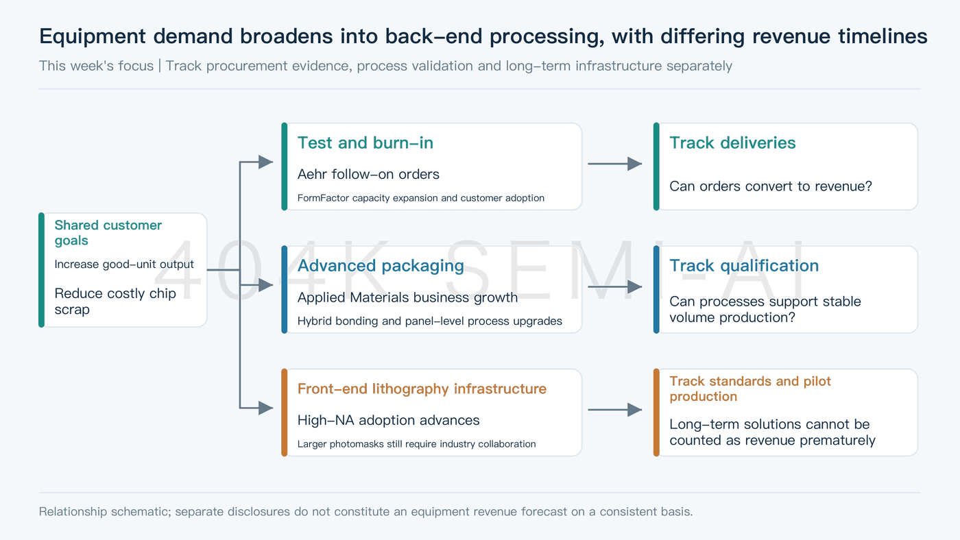
Investment priorities should start with customer purchasing behavior, followed by the economic cost of the problem each tool solves. A test system that prevents a high-value package from being scrapped at the final step has a clear purchasing rationale. Yet a simpler test flow could also reduce the number of systems required. A sound long-term demand thesis does not guarantee comparable orders or margins for every supplier.
This week’s most useful counterpoint came from monthly operating data: Taiwan’s advanced packaging equipment industry recorded slower year-over-year revenue growth in August than in July, while Grand Process Technology, Gallant Precision Machining and All Ring Tech remained ahead of quarterly revenue expectations based on their July–August performance. Slower growth and performance above expectations can coexist. Equipment analysis must distinguish actual revenue growth, prior market expectations and the durability of customers’ next purchasing cycle.
Front-End Wafer-Fabrication Equipment
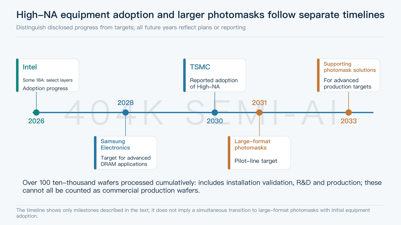
High-NA commercialization is shifting from demonstrating patterning capability to demonstrating economical volume production. Intel and ASML disclosed this week that the relevant systems have cumulatively processed more than 1 million wafers. That total includes installation qualification, R&D; and production wafers; it cannot all be treated as commercial chip output. Disclosed production use covers specific layers of selected 18A products, rather than a wholesale conversion of the process.
Intel said overlay accuracy, throughput and tool availability meet foundry expectations. These measures are more informative than cumulative wafer counts alone. For equipment buyers, better resolution can still produce a weaker return on investment if good output per hour falls. Track the breadth of production-layer use, sustained operating performance and customer qualification rather than extrapolating new tool demand from R&D; wafer volumes.
The dates on different companies’ roadmaps also refer to different milestones. Samsung Electronics and ASML target advanced DRAM applications in 2028; TSMC’s 2030 High-NA adoption timeline comes from reporting. The 2031 target for a larger-mask pilot line and the 2033 target for supporting solutions in advanced production are separate milestones. Earlier High-NA adoption does not imply a simultaneous transition to larger masks.
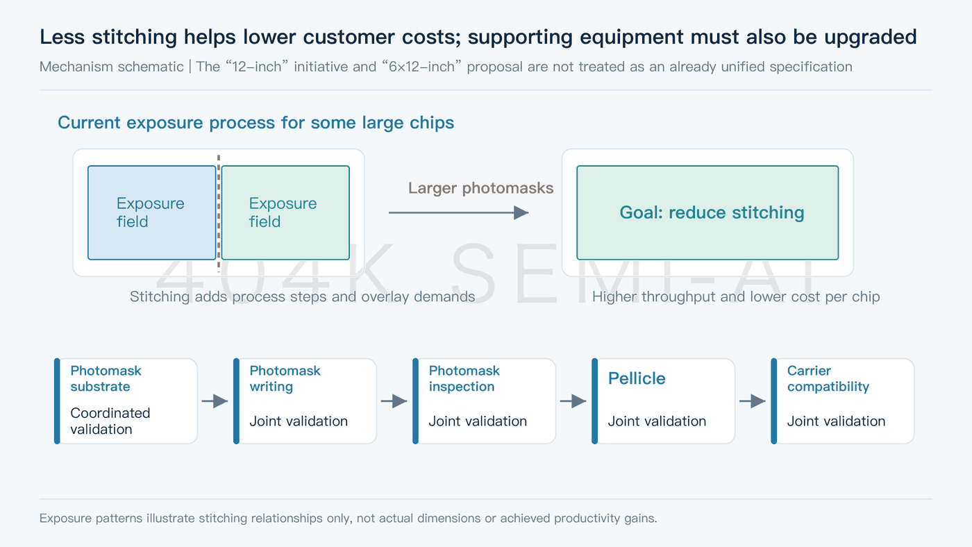
The larger-mask opportunity extends across the supporting equipment ecosystem. Current High-NA optics reduce the exposure field, potentially requiring stitching for large chips. Larger masks aim to reduce stitching, improve throughput and ease the associated overlay burden. ASML’s collaboration with TSMC brings broader industry participation to this long-term transition.
The supporting requirements span mask substrates, writing, inspection, pellicles and carriers, all of which must be compatible. Reports refer both to a “12-inch” initiative and to Intel’s “6 × 12-inch” proposal. These descriptions should not yet be treated as a unified final specification, much less used to calculate mask area, equipment counts or revenue growth.
Efficiency gains also work in both directions. Lower cost per chip may encourage broader adoption, while fewer exposures may deliver the same output. Equipment revenue ultimately depends on the combined changes in application layers, customer wafer volumes and productivity per tool. For mask inspection and handling suppliers, confirmed standards, prototype validation and customer purchases are closer to revenue realization than industry initiatives.
China’s front-end equipment sector offered process demonstrations and tender activity this week, but neither establishes volume orders. NAURA reportedly demonstrated a selective etch process for 64-layer 3D DRAM that removes silicon-germanium from a silicon/silicon-germanium stack while preserving the silicon structure. The equipment’s value lies in selectivity and uniformity within deep structures, indicating a potential extension of its etch capabilities.
Wafer validation, integrated-line yields, stable operation and maintenance costs still separate a process demonstration from sustained customer purchasing. Producing a vertical structure does not establish economical volume production of a complete device. NAURA’s progress should be assessed through customer adoption and repeat orders; the demonstration alone does not justify raising revenue forecasts.
Separate supply-chain reports on September 11 said CXMT’s new Shanghai fab had begun equipment tenders. Tendering is closer to purchasing than a distant fab proposal, but winning suppliers, tool configurations, delivery and acceptance remain unconfirmed. Reports also discussed expansion at other sites; their planned capacities should not be added together as equipment orders. Reports of TSMC’s 3nm expansion mentioned modifying and reallocating existing tools, another reminder that added wafer capacity does not translate entirely into purchases of new systems.
